Plasma chemistry,
made visible.
* OES · Plasma Process Chamber Monitoring
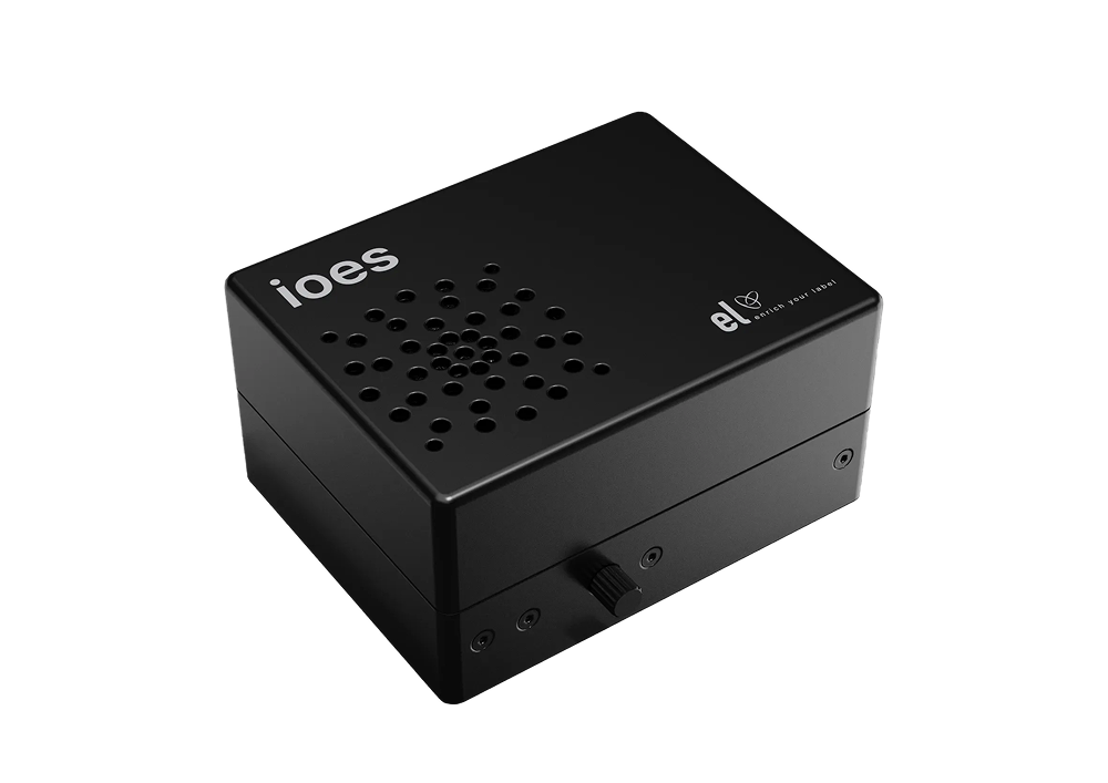
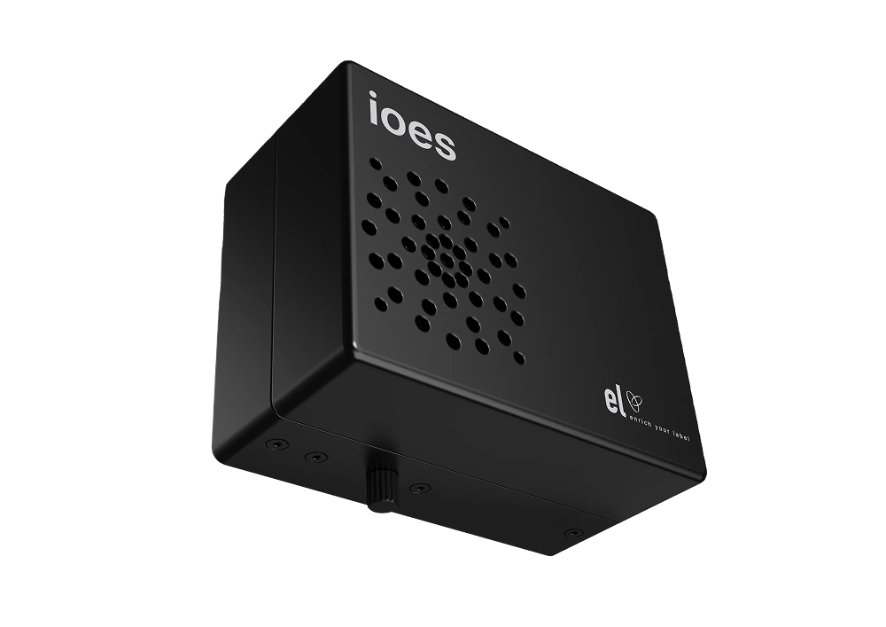
ioes uses Optical Emission Spectroscopy (OES) to analyze light emitted by plasma species inside process chambers — without contacting the gas stream. By monitoring spectral
intensity across 200–1050 nm, ioes tracks endpoint detection (EPD), plasma temperature, species concentrations, and real-time film thickness and refractive index of deposited layers
on wafers and glass substrates.
* Key Features
01
Non-Invasive In-Situ Monitoring
OES via optical fiber — no process gas contact, no contamination risk, no chamber modification beyond viewport access. The measurement is fully transparent to the process.
02
EPD + Film Thickness
Beyond standard endpoint detection, ioes simultaneously monitors the refractive index of wafer/glass and the thickness of deposited films from CVD process plasma emission — in real time.
03
Full UV–NIR Coverage
Wavelength range 200–1,050 nm (UV, VIS, and NIR options). Optical resolution 0.3–10 nm FWHM. Min. exposure time 1 msec. Covers virtually all plasma-relevant emission lines in semiconductor and display processes.
* Product Overview
Real-Time Plasma Monitoring with OES
ioes is an OES-based process monitoring system that analyzes plasma emission from ions and radicals inside process chambers. By monitoring specific wavelength
intensities in real time, it enables continuous observation of chemical species and process conditions. The system can simultaneously determine refractive index
and deposited film thickness, making it suitable for advanced CVD process monitoring. Following deliveries in 2021 and 2022, the third ioes system was supplied to
Samsung Display in 2025.
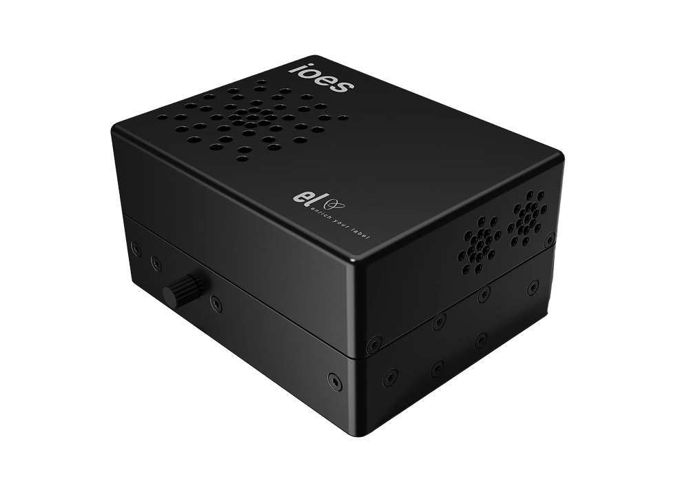
System Overview
Model / Principle
ioes / OES (Optical Emission Spectroscopy)
Detector
Sony ILX511 (UV Enhanced Coated)
Fiber Coupler
SMA905 or FC standard
Performance
Signal-to-Noise Ratio
> 250:1
Full Wavelength Range
200–1,050 nm
UV Range
200–450 nm
VIS Range
380–760 nm
NIR Range
550–1,050 nm
Optical Resolution
0.3–10 nm FWHM
Min. Exposure Time
1 msec
System Configuration
OS
Windows 10 (32/64-bit)
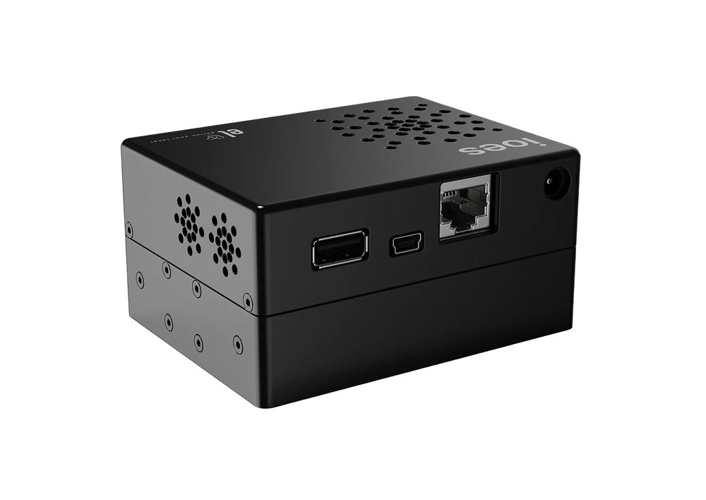
Installation Requirements
Dimensions (W×D×H)
90 × 70 × 44 mm
Weight
0.4 kg
* Applications
01
Etch Endpoint Detection (EPD)
Monitoring of etch process completion by tracking the appearance/disappearance of specific emission lines — the primary application of OES in semiconductor manufacturing.
02
CVD Film Thickness
Real-time monitoring of deposited film thickness and refractive index during CVD processes by analyzing plasma emission from the growing film environment.
03
Plasma Condition Monitoring
Continuous tracking of plasma temperature, species concentrations, and chamber condition throughout the process — enabling early detection of plasma instability or drift.
04
Chamber Cleaning Verification
Endpoint detection for plasma chamber cleaning processes by monitoring cleaning species (F-atoms, NF₃) and chamber cleanliness indicators simultaneously.
* Product
Related Products